


The technology will make self-driving cars and health checks possible by improving parts inside devices for faster and better wireless communication.
Self-driving cars that eliminate traffic jams, receiving a health diagnosis instantly without leaving home, or even feeling the touch of loved ones thousands of miles away might sound like science fiction. However, research led by the University of Bristol is bringing these possibilities—and more—within reach through advancement in semiconductor technology.
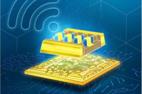
It is recognized that the transition from 5G to 6G will require an overhaul of semiconductor technology, circuits, systems, and related algorithms. For example, key semiconductor components—radio frequency amplifiers made from a material known as gallium nitride (GaN)—must become faster, more powerful, and more reliable.

The team tested a new architecture that propelled these GaN amplifiers to new performance levels. This advancement was made possible by discovering a latch-effect in GaN, which unlocks enhanced radio frequency device capabilities. These devices employ parallel channels that require the use of sub-100nm side fins—a type of transistor that regulates current flow through the devices.
The team piloted a device technology known as superlattice castellated field effect transistors (SLCFETs), which feature over 1,000 fins each less than 100 nanometers wide to drive current. While SLCFETs demonstrated top performance within the W-band frequency range (75–110 GHz), the underlying physics remained unclear.
The researchers identified the latch-effect in GaN as the key mechanism enabling the high radio frequency performance. To understand this effect in detail, the team combined electrical measurements with optical microscopy to locate the phenomenon. After analyzing more than 1,000 fins, the latch-effect was pinpointed to the widest fin.
To validate these findings, a 3D model was developed using simulation software. The next focus was to evaluate the latch effect’s impact on device reliability under practical conditions. Long-term testing confirmed that the latch effect does not harm device reliability or performance.
A factor contributing to this reliability was found to be a dielectric coating surrounding each fin. The latch effect was identified as a feature that can be harnessed for applications, potentially transforming aspects of daily life in the future.
Future work aims to increase the power density these devices can achieve, enabling higher performance and broader application. Collaboration with industry partners is planned to bring these devices to commercial markets.
Reference: Akhil S. Kumar et al, Gallium nitride multichannel devices with latch-induced sub-60-mV-per-decade subthreshold slopes for radiofrequency applications, Nature Electronics (2025). DOI: 10.1038/s41928-025-01391-5


