
The DC-DC converter design with 5V output, control options, protection features, and test support for fast and easy power project development.
NXP Semiconductors offers a full-bridge DC-DC switch-mode power supply reference design that demonstrates efficient power conversion using V series microcontrollers (MCUs). This converter operates as a transformer-isolated buck converter and consists of four primary stages: a full-bridge inverter, a transformer, a synchronous rectification stage, and an output filter.
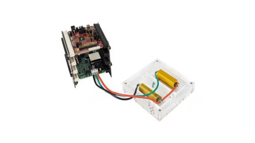
The Low-Voltage Full-Bridge DC-DC Switch-Mode Power Supply Tower board (TWR-SMPS-LVFB) serves as a peripheral module in the Tower System, providing a flexible development platform for rapid prototyping of various power-control topologies. By integrating two MCU/peripheral boards from the Tower System, developers can implement control strategies such as peak current mode, average current mode, and voltage mode control.

The full-bridge inverter converts the DC input into a high-frequency AC signal operating at 150 kHz. This AC signal is stepped down to the required voltage level by the transformer. On the secondary side, synchronous rectification converts the AC back to DC, and an LC filter smooths the output, delivering a stable 5 V supply capable of sourcing up to 8 A. The input voltage range for the converter is 20–30 V DC.
The design incorporates feedback circuits to ensure safe and accurate operation. A resistor divider network is used for voltage feedback, while a current transformer with a load resistor provides current feedback, both conditioned for MCU-level sensing.
To facilitate testing, the system includes a dynamic load circuit module. This allows users to evaluate different power-control techniques and demo software under various load conditions using a connected resistor at the output.
Key features of the design include:
- Input voltage range: 20–30 V DC
- Output current capability: up to 8 A
- Reverse polarity protection
- Full-bridge topology with transformer isolation
- Synchronous rectification on the secondary side
- Input: 20–30 V DC
- Has test load for fast load change tests
- Works with 4.5 V to 36 V supply
- Two drivers for IGBT or MOSFET use
- Has PWM control
The board also incorporates power rails derived from the main input voltage. A switching step-down regulator generates a 12 V rail (up to 500 mA), which powers the MC33269 linear regulator, the full-bridge MOSFET driver, and the synchronous MOSFET driver. From the 12 V rail, a 5 V linear regulator provides up to 800 mA for low-noise, simple-power applications. Additionally, a 3.3 V linear regulator, also capable of supplying up to 800 mA, powers both analog and digital circuitry, including onboard LEDs. Linear regulators are favored here for their simplicity in circuit design.
NXP has tested this reference design. It comes with a bill of materials (BOM), schematics, assembly drawing, printed circuit board (PCB) layout, and more. The company’s website has additional data about the reference design. To read more about this reference design, click here.


